CMOS Based Atom Chips for Sensor Applications
Ultra-cold atomic systems have proven over the last decade to be a excellent platform for the realization of quantum sensors, quantum computation or quantum simulation applications. A special implementation of this technology is the so called atom chip, where the magnetic fields generated by wires on a semiconductor chip will result in elaborated trapping potentials for the atomic ensembles. Atom chips show the potential to act as a scalable platform for quantum applications as soon as it is shown that this technology can be transferred to large scale production using established processes such as CMOS.
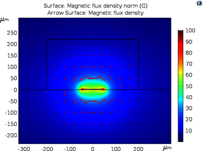
Within this work we will investigate the formation of magnetic fields using the MEMS module of COMSOL Multiphysics® for structures realizable using CMOS technology. Based on the obtained fields we will calculate the trapping potentials for the atomic ensembles and characterize the traps for parameters such as trapping frequency and power consumption.
Optimization in terms of thermal budget will be performed to find the ideal realization of CMOS based atom chips of which the first layouts will be presented
Download
- koller_poster.pdf - 0.72MB
- koller_abstract.pdf - 0.01MB